
Assistant Professor of Physics Perry Corbett has retrofitted one STM and repaired another. Corbett worked for the scientific research and technology company UES Inc. in conjunction with the AFRL, according to a news release from Miami University.
"Corbett, (Physics student) Nate Price, Lakshan Don Manuwelge Don and their colleagues will be able to map a sample's surface atom by atom using ultra-high resolution," states the release. "Corbett is in the process of modifying the STM to give it advanced capabilities, including adding a magnetic field as well as an additional chamber, which will allow Corbett's group to bring in samples from collaborators across the world."
Corbett can build STMs from scratch, draw a diagram from memory, or take them apart, screw by screw, Miami officials said.
"The microscope was in fantastic condition," Corbett said of the model that had been with the AFRL for about 12 years. "I had the tools in my toolbox to bring it back to life at Miami."
Price, who is from Edinboro, Penn., "worked with a more educational model of STM while at Brown, one that was less advanced but still produced interesting data," Miami's release said.
"We have a lot of different samples that we can look at under different conditions with an STM," Price said. "Hearing we were going to get one that can work at ultra-high vacuum and magnetic field strength with certain modifications we can make was really exciting."
"Corbett's expertise is in thin film growth and microscopy of magnetic, semiconducting and topological materials," Miami officials said. "In 2023, he received a near $800,000 grant from the National Science Foundation for his project, 'ExpandQISE: Track 1: A Deep-Dive into the Materials Science of Alpha-Ta Growth on Oxides for Superconducting Resonator Development'."
This fall, Corbett will mentor five Miami University undergraduates and five graduate students.
"My group focuses on both the growth and microscopy of materials," Corbett said. "We have a very robust training program to give people the skills needed for the semiconductor industry. They are immediately transferrable skills and a great opportunity for students."
Officials said Price's focus "is on the border between material science and quantum computing and how growing slight variations can change quantum properties and the way they hold information."
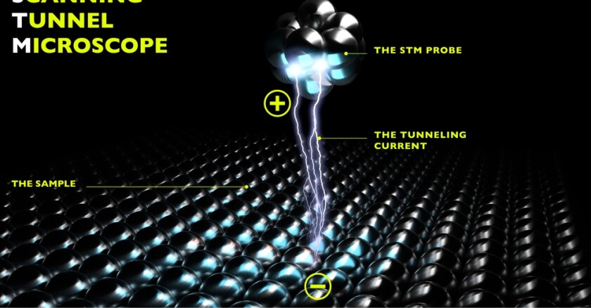
Using an STM will allow for incredible resolution, all the way down to the atomic lattice structure level, Price said.
"Those are not only incredibly helpful, but they are also some of the most beautiful images you can produce," Price said. "It's really all about resolution when it comes to an STM."
More collaboration could be in the works between Miami and the AFRL, and Corbett said positions are available in his group for interested students, according to the news release.
"There is good synergy here," Corbett said about Miami and the AFRL. "This is a great way for me to get the microscope back alive. They can send samples here, we can make measurements, and I can help train the next generation."
©2024 the Journal-News (Hamilton, Ohio). Distributed by Tribune Content Agency, LLC.